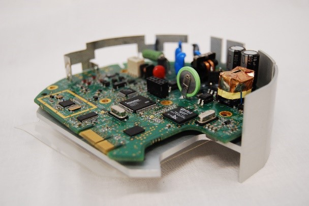
PCB Layout
- Rules Driven Designs (Design Constraints)
- Digital, Analog, RF, High Voltage
- Controlled Impedance and Matched Lengths
- .35mm uBGA to 2200+ pin BGAs
- Laser, Stacked, Buried via, via-in-pad, back drill
- High Speed (XAUI, PCIe, SerDes, LVDS, Fiber Channel, Gig-E, etc.)
- DDR2, DDR3, DDR4 memory
- Flex and Rigid-Flex Circuits
- Power Supplies, Heavy Copper
- FPGA/CPLD pin swaps, via minimization
- Stack-up development and verification
- Documentation and build packages preferred by Fab houses and CMs
- Designed for use from prototype to high volume production
- Sub-panel array optimization
- Schematic Capture
- Comprehensive Checking – design improvement feedback to get it right on the first REV
PCB Library Development
- Optimized IPC PCB Footprints
- Schematic Symbols
DFX Analysis (DFM, DFA, DFT, etc.)
Schematic and PCB Translations
- Altium Designer to OrCAD/Allegro
- OrCAD/Allegro to Altium Designer
- Design Reviews


Development Tools
PCB Layout Tools
-
- Cadence Allegro/orCAD PCB Designer
- Altium Designer
Netlist inputs from most front-end tools
Output Formats
-
- IPC-2581
- ODB++
- Fabmaster
- IDF 3-D Mechanical interface
- DXF
- Gerber RS274X
Schematic Capture
- OrCAD Capture
- Altium Designer
- Cadence ConceptHDL
Screen-sharing ensures rapid responses to questions and real time assistance with Design Review milestones

